And what makes IC’Alps more than a Design House
Discover what make ICAlps more than a Design House: our characterization lab dedicated to customer success.
IC’Alps’ characterization lab is a set of resources and expertise entirely dedicated to ASIC prototypes test campaigns. The lab engineer verifies that the actual performances of the integrated circuit are up to specifications. Like a test pilot, he also pushes the prototypes to their limits by any means necessary during the lab characterization. Finally, he identifies the root causes of any gap between the specifications and the actual measurements.

The design phase
However, the test campaign is only the end of a thorough preparation that started months before the actual tests.
First
designers carefully prepared their test sequences. They added observation points or paths in the ASIC and implemented dedicated test structures to ease the debug.
Precautions are different between digital and analog teams. In the analog field, any added path can bring additional parasitic and noise and degrade the performances measurements.
To allow the extraction of the exact performances that need testing, designers ran several simulations of their test sequences. While doing so, they also methodologically considered the test environment.
They want to ensure that they adequately test the performances in relation to the context and the goals.
Second
the characterization engineer prepared the test environment from a characterization plan defined together with the designers. Upon this plan validation, he moved on to the lab hardware preparation.
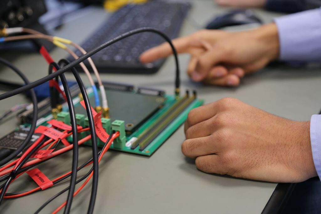
All resources for the characterization such as Source Measurement Unit, Oscilloscope, Arbitrary waveform generator or else must be calibrated and verified to ensure accurate measures. At same time, he specified, designed and subcontracted the fabrication of the test board to an IC’Alps QMS approved supplier.
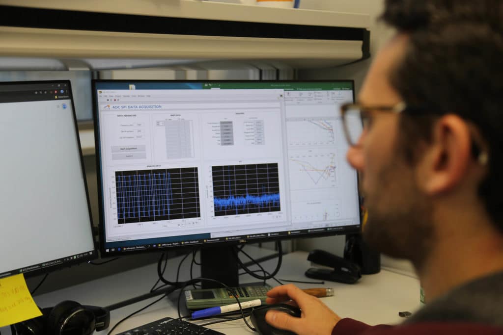
Finally, he developed all the test software required to drive the different equipment to be automaticaly executed by a test sequencer. He will repeat this work for each characterization.
A successful characterization is primarily a matter of preparedness from the team. Communication between all stakeholders is thus paramount and the project manager plays here an important role in coordinating all the effort toward achieving a successful characterization campaign.
The validation plan is designed hand-in-hand with the Customer.
Both the ASIC Designer and the Customer will run a characterization of the prototyped ASIC. The Customer will run his characterization in an applicative test environment. But IC’Alps will run his in a “standalone” environment meaning that we will test the ASIC on its intrinsic qualities and performances.
Waking-up the ASIC
When the circuit finally arrives after months of preparation, our lab engineer takes the lead to handle those measurements, supported by the principal designers. A critical phase begins with the sanity checks of the characterization environment with the first circuits.
At this point, the atmosphere can go up and down in a couple of minutes.
The lab engineer is monitoring the different signs that could prevent the circuit from working as expected. Any short-circuits or unusual power consumption? Can he write registers or access the integrated circuit via the Serial Peripheral Interface (SPI) embedded for this purpose?
Designers continue to play a role by analyzing the configuration registers, checking the first readings, and setting the right simulation corner thanks to the Process Control Monitoring (PCM) data provided by the foundry.

The characterization campaign
As soon as the power-up sequence is successful, the characterization can start.
Designers and lab engineer continue to work closely together to get and analyze the results of the first circuits and to adjust the test sequence when required. In the meantime, the project leader ensures a good and straightforward communication inside the team.
At the beginning of the campaign, all measurements are performed manually to ensure that the environment, test sequences or ASIC function do not have any impact on the readings. However, as soon as this phase is over, the lab engineer gradually automates the readings for considerable efficiency gains.
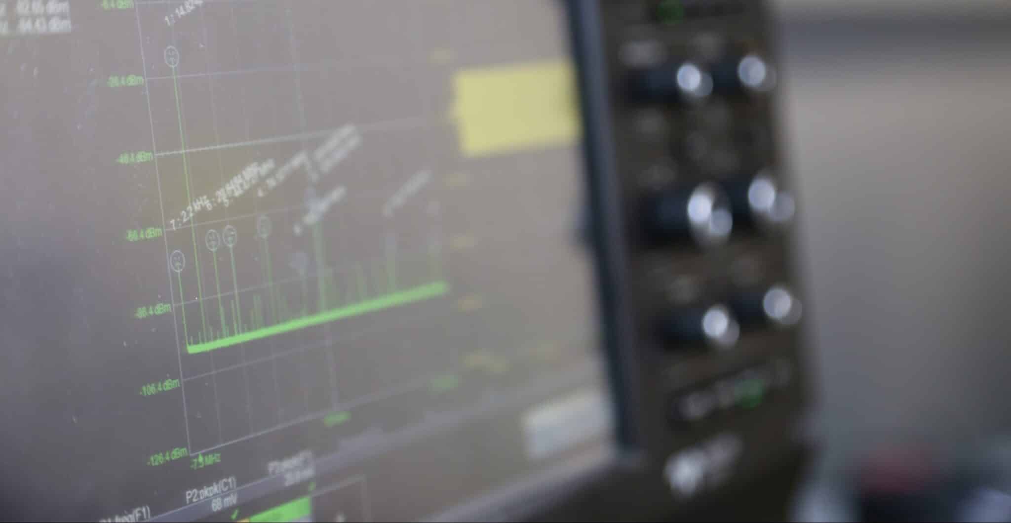
His role now is to compare the raw data generated by the ASIC with the specifications and the simulated data with one question in mind: does the circuit performance match the specifications?
This question have several answers according to the primary function of the circuit: power efficiency for a Power management system, steady performance under variable operating temperature, amplifier offsets and noise ratio, amplifiers gain, bandwidth.
As ASICs are custom-made, scrutinized specifications and performances can vary for the same application.
With those raw data, designers can correlate the measurements with the simulation result and fill the gap between the two.
Full support beyond GDSII
Going through the validation plan, the lab engineer has extracted all the integrated circuit characteristics. Designers can request additional tests but the circuit’s behavior will likely not present any more surprise.
The lab engineer and designers compile all results in a characterization report. This will allow the Customer to get an overview of the actual performances measured on silicon of the first prototypes and to compare those results with the one reached in the application environment.
From now on, if the Customer validates the prototype as it is, the next step is to move forward to the industrialization by preparing the industrial test software and hardware. In any cases, IC’Alps is fully comitted until our customers’ products reach their markets and start the associated production.
This is what make ICAlps more than a Design House: our characterization lab dedicated to customer success.

