Set of primary blocks we use when designing your ASIC/SoC
Set of primary blocks we use when designing your ASIC/SoC
By using them as they are or modify them to fit customer’s needs, our team improves performance & design time and helps offer differentiated IC architectures. It reduces development risks and costs while contributing to first-time-right project execution.
Overall, this approach allows IC’Alps to better serve our customers when designing their ASIC/SoC.
We develop our own IP component library to assess the reachable performance and gather experience for future ASIC integration.
Our IP solutions have been silicon verified in one or more technological nodes and are scalable and portable with respect to foundry’s specific manufacturing process.
The following in-house IP components are available to our customers to complement our third-party IP partnerships.
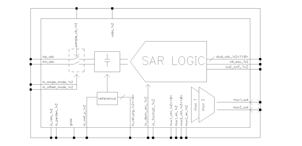
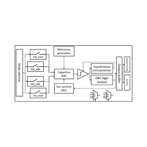
12-bit general purpose Analog-to-Digital Converter (ADC) with a sampling rate up to 1-MSPS.
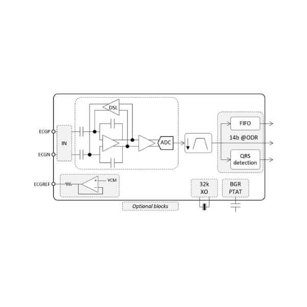
Ultra-low power analog front-end (AFE) readout circuit designed for wearable and implantable medical devices. Clinical-grade electrocardiogram (ECG) waveforms and QRS detection
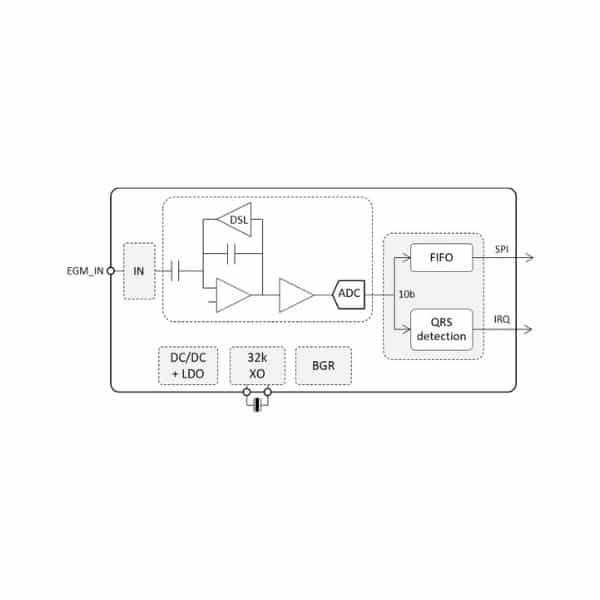
Nanopower unipolar acqusition chain for intracardiac pacemaker
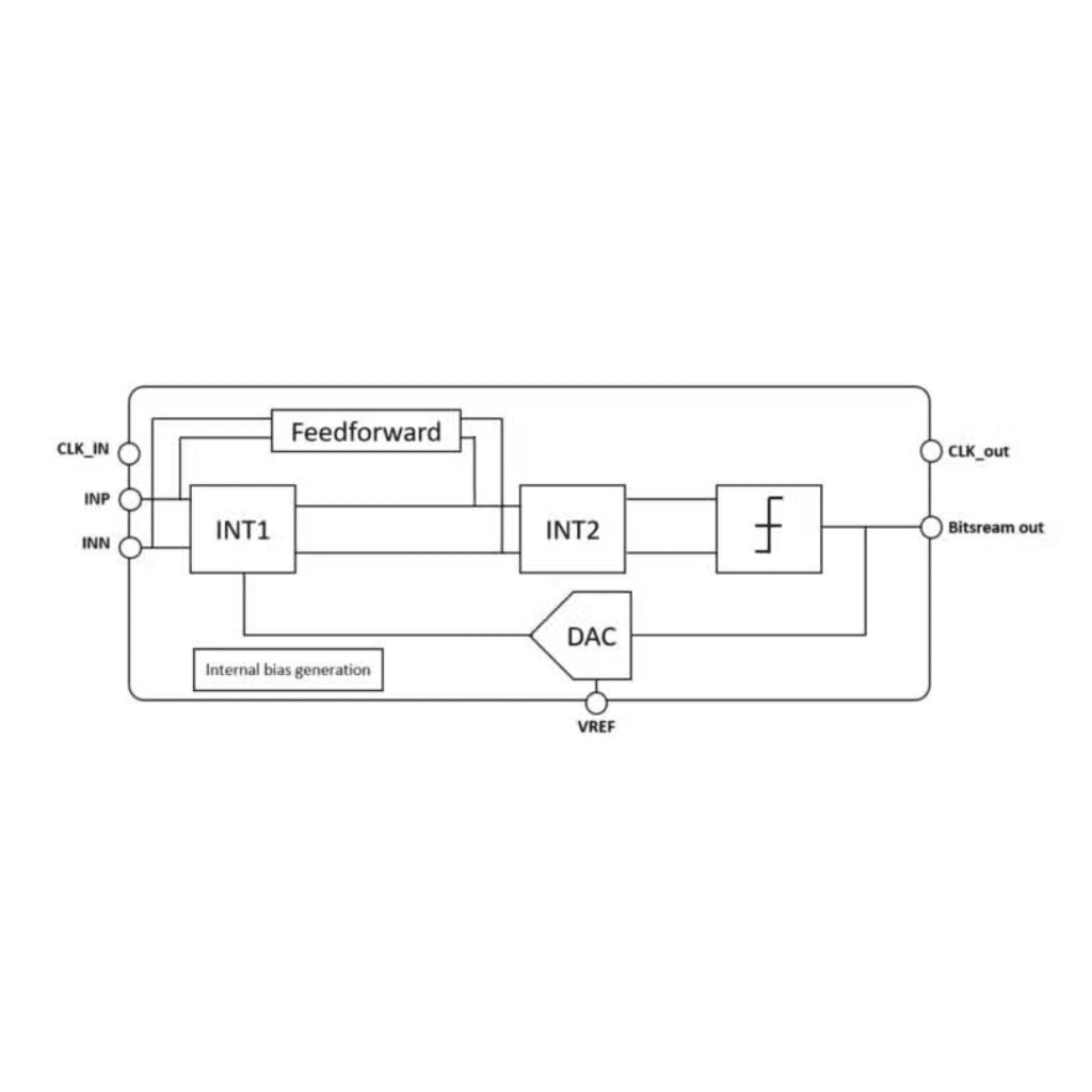
SDM18 is a second order single-loop, single-bit, delta sigma modulator optimized for low power consumption applications.
We provide the soft IP and required expertise to uniquely combine hardware security features and low-power in a custom ASIC solution for the needs of IoT and medical applications, or more generally serving the need of unique identifier (such as a fingerprint) in either FPGA or ASIC technologies.
Our TRNG and PUF are based on asynchronous solutions, using only standard cells (no specific cells or memories), and providing performances (bit rate generation) > 100x than classical SRAM-based solutions
Through capitalization of our IP library and re-use of standard blocks
Compared to full in-house design
With silicon proven subsystems
Across a variety of technologies